A Low-Cost FPGA/SDR Testbed for Power Amplifier Characterization
Overview
This post summarizes the measurement testbed described in our paper “A Comparison of Surrogate Behavioral Models for Power Amplifier Linearization under High Sparse Data” (Sensors, 2022, 22(19), 7461). The goal of the setup is to capture real RF measurements from a power amplifier (PA) under test, so that behavioral models — and the digital predistortion (DPD) that linearizes the PA — can be trained and validated against hardware rather than simulation alone.
Instead of relying on expensive dedicated RF instrumentation, the testbed is built around a software-defined radio (SDR) running on an FPGA system-on-chip. This keeps the platform affordable and reproducible while still supporting wideband signals and the acquisition of crest factor reduction (CFR), PAPR, and ACPR measurements at different instantaneous bandwidths.
Testbed Architecture
The testbed is organized in two stages:
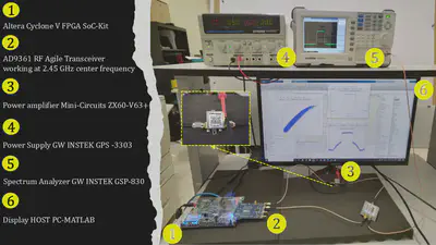
- Digital stage (FPGA/SDR). A Cyclone V FPGA SoC kit hosts the SDR. An embedded Linux running on a Microblaze/ARM (Zynq) architecture uses the Analog Devices
libiiolibrary to provide a full-duplex link between the host PC (MATLAB) and the FPGA. Baseband waveforms are streamed from MATLAB, stored in the FPGA’s DDR memory, and exchanged over a standard Ethernet connection. An AXI interconnect provides the low-latency, high-throughput data path on-chip. - Analog/RF stage. An AD9361 RF transceiver up-converts the baseband signal with a quadrature modulator driven by an internal local oscillator set to 2.45 GHz, generating the stimulus that drives the PA. A feedback path routes the PA output through a power splitter to a spectrum analyzer for frequency-domain measurements.
The transceiver uses direct conversion with 2×2 I/Q channels, a 320 MSPS DAC and a 640 MSPS ADC, and a 128-tap interpolation FIR filter with an adjustable internal sampling rate.
Device Under Test and Instrumentation
- Power amplifier (DUT): Mini-Circuits ZX60-V63+, a 50 Ω coaxial gain block biased at 5 V, with roughly 20 dB of gain at 2.45 GHz (measured at 18.79 dB for the LTE-10 MHz signal and 18.45 dB for LTE-15 MHz).
- SDR / transceiver: Analog Devices AD9361 Agile Transceiver (ARRadio / AD-FMCOMMS3-EBZ card).
- FPGA: Altera Cyclone V SoC kit.
- Power supply: GW INSTEK GPS-3303.
- Spectrum analyzer: GW INSTEK GSP-830.
- Host: PC running MATLAB.
Measurement Workflow
Test signals are single-carrier 64-QAM multiplexed over OFDM, following LTE at 10 MHz and 15 MHz bandwidths. Before each run, the system is calibrated so that a properly synchronized signal reaches the PA input, with the calibration power set for both peak and average levels at the PA output.
Captured, real-valued I/Q data are post-processed in MATLAB using the LTE Toolbox and RF Blockset models to compute the key figures of merit: NMSE, PAPR, ACPR, and CCDF. These measurements feed the training and testing of the surrogate behavioral models compared in the paper.
Why a Low-Cost Setup Matters
By combining an FPGA-based SDR, an inexpensive commercial PA, and budget-tier bench instruments, this testbed delivers a complete, reproducible PA characterization and DPD-validation flow at a fraction of the cost of a traditional instrument rack. It lowers the barrier for research and teaching in RF linearization, where access to high-end vector signal generators and analyzers is often the limiting factor.

Jose Alejandro Galaviz-Aguilar, Ph.D.
RF Research & Development Engineer
My research interests include RF power amplifier linearization, digital predistortion, behavioral modeling, and FPGA-based DSP systems.